 Chip Services

 Products
- Automotive and Industrial control
- Information Security
- Edge Computing& Network Communication
Products

 Resources

 Language

CUni360S is an information security chip applicable to contact IC, contactless IC and magnetic strip cards. It is designed based on the 32-bit security CPU CS0 with independent intellectual property rights. CUni360S is distinguished by low power consumption, high performance, multifunction and high security level. It can be widely used in IoT, POS machines, dual-interface card readers, dynamic QR code terminals, and other fields. The chip’s typical operating frequency is 80MHz.

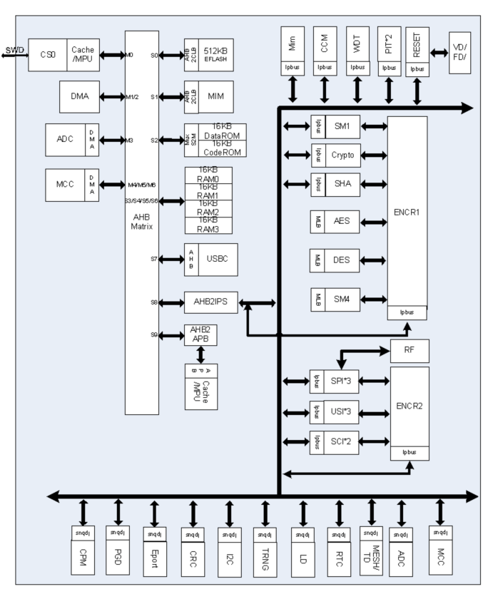
Block diagram of CUni360S
● 32-bit low-power RISC core with highly optimized 3-stage pipeline
● Supporting byte, half-word, and word memory access
● Supporting interrupt nesting
● Supporting single-cycle 32-bit x 32-bit hardware integer multiplier array, 3 to13 cycle hardware integer frequency divider array
● Memory protection unit (MPU)
● Low power consumption and high performance
● Supporting Cache
● Timing module EPT
● 64K bytes of SRAM
● 16K bytes of ROM
● 512K bytes of EFLASH. 512 bytes/Page, minimum 100,000 erase cycles
● DMA/EDMA
● 2 timers (PIT)
● Watchdog (WDT)
● Real-time clock (RTC)
● Time counter (TC)
● Asymmetric algorithms
- 1024bit RSA
- 2048bit RSA
- 256bit SM2 prime field
● Symmetric algorithms
- DES/3DES supports ECB/CBC mode
- AES supports ECB/CBC/CTR mode
- SM4 supports ECB/CBC mode
● Hashing algorithms
- SM3
- SHA-0/ SHA-1/ SHA-224/ SHA-256/ SHA-384/ SHA-512
● CRC
- Supporting CRC32/ CRC16/ CRC8
- Supporting DMAC operation
● Memory protection mechanism
- Application-oriented memory partitioning with hardware support for secure isolation
- Scrambling bus
● True true random number generator, compliant with FIPS 140-2 standards and national commercial cryptography standards
● Safety detection and protection unit
- Voltage detection unit
- Light detection unit
- Power supply burr detection unit
- Metal shielding protection
- Temperature detection unit
- Frequency detection unit
- Physical detection protection
- Clock and reset pulse filtering
- Optimizing wire routing for security
● PCI certification satisfaction
- Supporting 128 Byte NVSRAM
- Supporting 4 pairs of open cover detection signals, configured with dynamic/static detection mode
- Supporting voltage detection
- Supporting temperature detection
- Supporting self-destruct and clear NVSRAM
● Unique serial number for each product
● Main power input voltage: 1.9V~5.5V, PCI domain input voltage: 1.9V~3.63V
● Typical power consumption: 20mA @ 60MHz, low-power Sleep mode: less than 50uA
● ESD: 2000V
● Supporting internal power-on reset and external reset
● QFN76
● QFN68
● Level II of security chip for commercial crypto product certification
● Security assessment of personal payment terminal chip;
● IoT chip security test of smart Cloud Testing
● Application function test of Smart Cloud Testing ID2

● IoT
● Dual-interface card reader
● POS
● Personal payment terminal
● ID card reader
● Dynamic QR code terminal

? Complete development environment
? Rich driver libraries
? Complete application solutions